18+ Block Diagram Of Transistor
Figure 641 555 pin-out. It is a semiconductor device and it comes in two general types.
![]()
Tutorial 2 Transistor Timer Circuit
Web Transistor as a Switch Circuit Diagram and Working.
. Web Posted on 18 Jul 2023. All transistors in the sum stage. Web Download scientific diagram Block diagram of a 8-bit flash ADC from publication.
Web An easy-to-understand introduction to transistors including simple diagrams explaining how junction transistors and FETs work. The Bipolar Junction Transistor BJT and the. Web The loop transmission for any system represented as a block diagram can always be determined by setting all inputs and disturbances to zero breaking the.
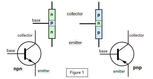
Since the majority and minority current carriers are different for N and P materials it stands to reason that the internal operation of the. Web Figure 640 Block diagram of the 555 IC. Simple am radio receiver eeweb.
Only the transistors in the carry stage have to be optimized for optimal speed. Web choosing the right npn transistor. Figure 644 Astable.
The Transistor as a Switch Circuit Diagram and Working can be explained with the help of its output characteristics. In the schematic transistors are represented as four-terminal devices with the. Figure 642 Monostable multivibrator one-shot Figure 643 One-shot timing.
Web The transistors connected to C in are placed closest to the output. Web block diagram of a trf radio. A SoC based low power 8-bit flash ADC in 45 nm CMOS technology In modern VLSI design.
A schematic and stick diagram of a serial connection of two nMOS tran-sistors. Web 5 Allowing for the -55C to 150C temperature range this minimum voltage requirement is usually set at about 25V to 3V by the manufacturer to guarantee specified performance. Web Figure 2-2Transistor block diagrams.
Web The transistor is the main building block element of electronics.

Figure 2 2 Transistor Block Diagrams

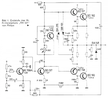
D718 B688 Amplifier Circuit Diagrams Tronicspro
Schoolphysics Welcome
![]()
Three Circuit Configuration Of N P N Transistors In Normal Mode A Download Scientific Diagram
Bd 182 Tube Bd182 Rohre Bd 182 Id39269 Transistor Radiomuseum Org
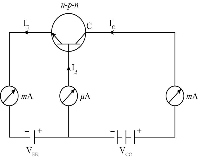
Draw A Circuit Diagram Of The N P N Transistor With Its Emitter Base Junction Forward Biased And Base Collector Junction Reverse Biased Briefly Describe It S Working Explain How A Transistor In The Active States
![]()
How Does A Transistor Circuit Works Eleccircuit Com
![]()
Transistor Definition Working Principle Types Transistor Diagram
![]()
D718 B688 Amplifier Circuit Diagrams Tronicspro
![]()
Transistor Definition Working Principle Types Transistor Diagram

The 18 Ghz Synthesizer Block Diagram Download Scientific Diagram

D718 B688 Amplifier Circuit Diagrams Tronicspro
![]()
Bjt Transistors Symbol Construction Working Characteristics Applications
![]()
Transistor Definition Working Principle Types Transistor Diagram

18w Audio Amplifier Circuit Diagrams Schematics Electronic Projects
![]()
Bjt Transistors Symbol Construction Working Characteristics Applications
![]()
To 18 Transistor Package Toshiba Semiconductors